Customization
▶ Custom sensor development
▶ Optical characteristics customization
▶ Shape/performance customization
▶ Modularization/OPIC conversion
▶ Bare chip assembly
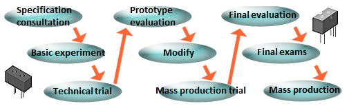
Custom sensor development
The flow of custom sensor development is as figure below.
 |
Developing a custom sensor is not as difficult as you might think.
Ultimately, the issue is "easy to use" or "difficult to
use".
You only need to contemplate about some minor situations.
After that, we will complete the long-awaited, "easy to use"
sensor that incorporates our expertise.
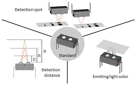
Optical characteristics customization
There are various things to detect.
For example, there are various types such as thin paper, thick paper, those
that allow some light to pass, and those that do not pass at all.
The standard product may not meet your desired detection characteristics.
In such cases, we hear your requests, and based on our standard products,
we will customize the optimal optical characteristic sensor for your equipment
and provide products that satisfy the desired characteristics.
We will narrow down the characteristics by the following methods according
to your request.
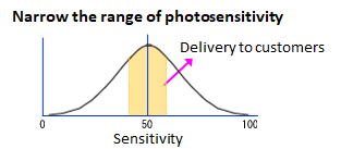
![]() Narrow the range of photosensitivity
Narrow the range of photosensitivity
Narrow the light receiving sensitivity range by utilizing the selection
products of LED and light receiving bare chip.
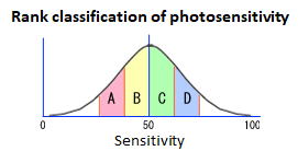
![]() Rank classification of photosensitivity
Rank classification of photosensitivity
By classifying the sensitivity of optical sensors for large variations,
we contribute to increasing the yield of customers.
 |
 |
|
 |
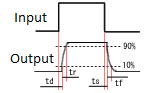
![]() Improved response time
Improved response time
We will improve the response time by custom quick responsive photo detectors
and processing circuit designs.
 |
 |
Custom photo IC |
![]() Expansion and reduction of the detection range
Expansion and reduction of the detection range
We will answer the customer's request for the detection range by optical
lens design, squeezing slit, etc.
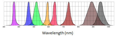
![]() Limitation of light emission and detection wavelength
Limitation of light emission and detection wavelength
The wavelength is limited by the wavelength selection of bare chips and the use of filters.
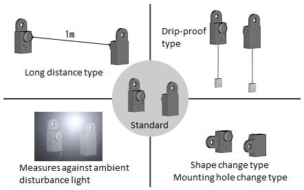
Shape / Performance customization
We will make custom products according to the customer's detailed request, such as "A little smaller one", "Opposite direction mounting holes", "Type of connectors not to fit", etc.
| ・ Reflective type |
 |
| ・ Separate type |
 |
| ・ Transmissive type |
| |
Modularization / OPIC conversion
There are many troublesome tasks such as ordering requests for each part, delivery date management, and production planning for mounting the part.
Also, the delivery of ordered products is often delayed. You may be worried about the urgent demand for each delivery and the troublesome work of rebuilding the production plan.
We will procure the optical sensor, electronic components for driving the optical sensor, mechanical parts, PCB, etc, which are commonly individually procured by the customer, in a lump and modularize them to reduce the customer's procurement cost and shorten the delivery.
Of course, all items are shipped after "characteristic/appearance inspection".
 We procure needed parts |
 |
 Modularization |
|
Photo IC conversion |
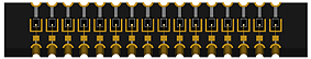
Bare chip assembly
Normally, when using sensor parts, we will use various parts sold by each manufacturer to create products.
Therefore, if 10 LEDs are mounted side by side as example, even if SMT components are used, each LED has its own housing and take space, so it may make the product large.
The "bare chip assembly" is recommended in such cases.
The bare chip such as LED, photodiode, OPIC, etc. is die-bonded directly to the PCB, and their electrodes and the board are connected by wire bond.
This makes it possible to produce products that are much smaller, thinner, and more space-saving than mounting each component side by side.
For the PCB design, of course, we will surely design a pattern that meets the customer's request.
This is a method that saves space and reduces costs.
Please consider it.
 |
|
 |
|
 |
|
 |
| Substrate cleaning | Die bond | Wire bond | Junction coat |
・ Custom example
 |
 |
|
| LED array | Large size bare chip SPD | Multi-split SPD |
 |
||
| PD array (1mm pitch between chips) |
OPIC bare chip | |